| GISdevelopment.net ---> AARS ---> ACRS 1999 ---> Poster Session 5 |
A Method of Measuring
Anti-Radiation Performance for Optoelectronic Components Applied in the
Irmss of Cbers
Zhang Xuhui, Wang
Shitao
(Beijing Institute of Space Machine & Electricity, Beijing, 100076
Abstract (Beijing Institute of Space Machine & Electricity, Beijing, 100076
This paper presents a practical electrical- measuring method with the help of mechanical means through which the effect on the Optoelectronic components caused by space radiation can be measured qualitatively and quantitatively by the from of electric signal.
In this paper, the simulated space radiation environment, the working state of the components and the test requirements are described in detail. The block diagram of the measurement circuit, the schematic drawing of the measurement assembly and results of measurement are given.
Besides, concrete application of optoelectronic components in the IRMSS (Infrared Multi-spectral Scanner) is briefly described in this paper.
Introduction
All space instruments must be adapted to radiation environment in their service life. Different radiation has different effect on the space instruments. Optoelectronic components are widely used in optoelectronic techniques, but they are limited to be used in space because of the radiation performance of optoelectronic components. The method study of measuring anti-radiation for optoelectronic components is carried out around tueir concrete application in the IRMSS of CBERS (China-Brazil Earth Resources Satellite)
Each optoelectronic component has both optical and electrical features, which make it special to measure its anit-radiation performance. The component here refer to luminescent and photosensitive units. This paper presents a practical electrical-measuring method with the help of mechanical means through which the effect on the Optoelectric components caused by space radiation can be measured qualitatively and quantitatively can be measured qualitatively and qualitatively by the form electric signal, and the results of measurement are the basis of taking anti-radiation protection measures and design.
2 Anti-radiation performance measurement of optoelectronic components
2.1 Radiation environment
Cobalt radiator which is isotropic is used to simulate the space radiation environment (y-ray), the radiative dose is accumulative while counted.
2.2 The block diagram of the measurement circuit and the schematic drawing of the measurement assembly.
2.2.1 The block diagrams of the measurement circuit, see figure 1.
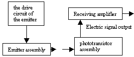
Figure 1: The Block Diagram
2.2.2 The schematic drawing of the measurement assembly, see figure 2.
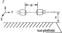
Figure 2 the schematic Drawing
2.3 Test requirements
2.3.1 The working states of the components
The measured working states in radiating field and monitored during radiating process by radiation resistant cable see figure 3
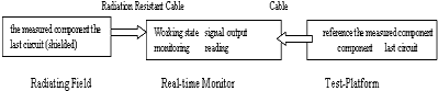
Figure 3 The Test Scene
Notes: the phototransistor has two working states which are linear and saturate states. The two working states are available by regulating the stop of emitter or phototransistor or by magnifying the luminosity of the emitter.
If the phototransistor works in deeply saturate sector, the variety of its parameters can only be measured qualitatively, only in linear sector can it be measured quantitatively.
2.3.2 The requirements to the emitter and the phototransistor assemblies
The emitter and phototransistor assemblies are on the test-platform, the distances from the central axis of the emitter (Y direction) to the platform and from the central axis of the phototransistor (Y direction) to the platform are equal ( in Z direction, expressed as "h"). The contact planes of the assemblies with the platform have the required planeness which makes the maximum of signal output invariant makes the maximum of signal output invariant while the emitter and phototransistor assemblies are moved each other on the platform in x direction. The distance (d) should be kept constant when assembly is moved.
Reference phototransistor is used while the emitters are measured.
Conversely, reference emitter is used while the phototransistor are measured.
The reference component assemblies are mounted on the platform.
2.4 Measuring method
Being reference of each other, the emitter and phototransistor are made to coupling pair, forming the relation of cause and effect, then the maximum of signal output can be compared before and after radiation (an example for phototransistor is given below)
Before radiation, the reference emitter is made to be in required working state, the maximum of signal output Vimas can be read out by moving the measured assembly in X direction.
After radiation, take out the phototransistor assembly from the radiating field and align it with the reference assembly, then the maximum. of signal output V2mas can be read out by reset measurement.
The emitter can be measured using the method mentioned above.
2.5 The results of measurement
The results of measurement can be calculated according to the formula below:
For the emitter, the variety of its parameter is
| K1 | V2mas -
V1max ---------------- V1max |
x 100 % |
K1 is the factor between the optical and electrical parameters.
For the phototransistor, the variety of its parameter is
The curve diagrams show that the anti-radiation capabilities of the emitters and phototransistors are decreased in turn arranging in the order number (1)(2)(3).
3 The application of optoelectronic components in the IRMSS
The application of optoelectronic components is involved in many places with different model type and working states in the IRMSS of CBERS.
| K2 | V2mas -
V1max ---------------- V1max |
x 100 % |
or
| K3 | V2mas -
V1max ---------------- V1max |
x 100 % |
V1max - the initial maximum of signal output (V),
V2max- the maximum of signal output after radiation (V),
V0 - the value of the linear dynamic range of signal output (V).
Note : The value of the linear dynamic range of signal output is related to the component itself and the test circuit.
The relations between the variety of signal output following radiative dose of emitters and phototransistor during radiation are given below, see figure 4 and figure 5.
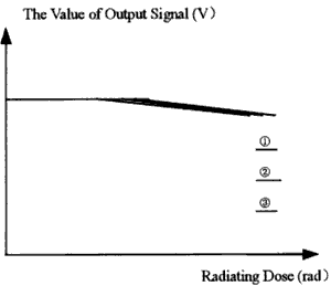
Figure 4: The Curve for Emitters
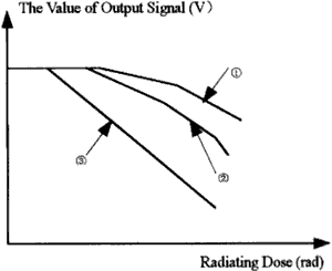
Figure 5: The Curve for Phototransistors
In the SMA (Scan-mirror Assembly), the coupling pairs formed by optoelectronic components and logical circuit supply the IRMSS with forward, backward and forward-to-backward scanning position signals. The switching characteristic of the components is used here. Whether liner or saturate sector the phototransistor works in, the design requirements can be met if the coupling pairs meet the needs of logical circuit after radiation.
The optoelectronic components in the SLC (Scan-line Corector) and the RLD (Revolving Light Diaphragm) are used the same way as the SMA. The SLC and shutter position signals which are synchronous with scanning signals which are synchronous with scanning signals will be available after frequency-lock and phase-lock circuits in this application.
Emitters are first used to be light source of the optical system in the SAM (Scan-angle Monitor) which can supply the IRMSS with standard dynamic scan-angle position signals. The variety of signal output must be measured definitely after radiation in this application.
The anti-radiation performance of the optoelectronic components can be measured with their applied circuit by developing the study of measuring method, and the results of measurement are feedback to the design itself, then the working margin and reliability of the system may be improved with components choosing, anti-radiation protection and signal compensating measures.
4 Conclusion
The anti-radiation capabilities of optoelectronic components are different because of their different materials and manufacture techniques.
The measuring method mentioned above is in common use and can be widely applied to luminescent units, photosensitive units or their combination.
In the IRMSS, all subsystems in which optoelectronic components are used have met the operating demands.